
Output Characteristics of n-channel JFET 
Theory
Introduction:
The n-channel Junction Field Effect Transistor (JFET) is a type of FET where the current conduction is due to electrons, making it a unipolar device. The operation of an n-channel JFET relies on the control of the current flowing through a channel of n-type semiconductor material by the voltage applied to the gate terminal. The primary regions of operation are determined by the relationship between the gate-source voltage (VGS) and the drain-source voltage (VDS), influencing the device's output characteristics.
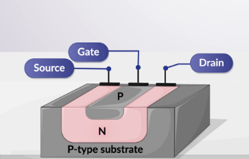 **Fig. 1. Threshold Voltage and Inversion charge**
Structure and Operation
An n-channel JFET consists of a channel of n-type semiconductor material with p-type regions diffused on either side, forming p-n junctions. These p-type regions are connected to the gate terminal, while the n-type channel connects the source and drain terminals. When a voltage is applied between the drain and source (VDS), electrons flow from the source to the drain, constituting the drain current (ID).
Gate-Source Voltage (VGS) Influence
The gate-source voltage (VGS) is crucial in controlling the channel's conductivity. For an n-channel JFET, a negative VGS depletes the channel of electrons, reducing the current flow. When VGS is zero, the JFET operates at its maximum current for a given VDS. As VGS becomes more negative, the channel narrows, restricting the current flow until the channel is completely pinched off, and the current becomes minimal.
Regions of Operation
Ohmic (Linear) Region
- In this region, the JFET operates like a variable resistor. The VDS is low, and the channel is uniformly conductive.
- The drain current (ID) increases linearly with an increase in VDS.
- The relationship can be approximated by Ohm's law: ID ≈ VDS / RDS(on), where RDS(on) is the on-resistance of the JFET.
Active (Saturation) Region
- As VDS increases, the channel near the drain end starts to pinch off when the voltage at the drain end of the channel equals the gate voltage plus the pinch-off voltage (VP).
- The current ID saturates and becomes relatively independent of VDS. The JFET enters the saturation region where ID is controlled by VGS and is given by: $$I_D = I_{DSS} (1 - V_{GS} / V_P)^2$$ where IDSS is the drain-source saturation current and VP is the pinch-off voltage.
Cutoff Region
- When VGS is sufficiently negative, the channel is fully depleted, and the JFET is off. The drain current (ID) is almost zero.
Breakdown Region
- If VDS exceeds a certain critical value, the JFET enters the breakdown region where the drain current increases rapidly with a small increase in VDS. This is due to avalanche breakdown of the p-n junctions and can potentially damage the device.
Output Characteristics Curves
The output characteristics of an n-channel JFET are graphically represented by plotting the drain current (ID) against the drain-source voltage (VDS) for various gate-source voltages (VGS). The typical output characteristics curves can be divided into different regions as described above, showing how ID varies with VDS for different VGS levels. These curves illustrate the JFET's behavior under different operating conditions and are essential for circuit design and analysis.
Mathematical Model
The mathematical model for the output characteristics in the active region is given by the Shockley equation:
$$I_D = I_{DSS} (1 - V_{GS} / V_P)^2$$
where IDSS is the drain-source saturation current when VGS = 0, and VP is the pinch-off voltage. This quadratic relationship highlights the sensitivity of ID to changes in VGS, emphasizing the importance of gate control in JFET operation.
In summary, the theory behind the output characteristics of an n-channel JFET involves understanding the influence of VGS and VDS on the drain current (ID). By analyzing the different regions of operation and their corresponding behavior, one can effectively utilize the n-channel JFET in various electronic applications, ensuring optimal performance and reliability.
The expression for the drain current of a n-channel JFET in the linear regime is,
$$\begin{equation} I_D=I_p\left[\frac{V_D}{V_p}-\frac{2}{3}\left(\frac{V_{bi}+V_D-V_G}{V_p}\right)^{3/2}+\frac{2}{3}\left(\frac{V_{bi}-V_G}{V_p}\right)^{3/2}\right], \end{equation}$$
where,
$$eV_{bi} = k_B T \ln \left(\frac{N_A N_D}{n_i^2}\right) \qquad n_i = \sqrt{N_c N_v \left(\frac{T}{300}\right)^{3}} \exp\left(\frac{-E_g}{2 k_B T}\right).$$
In the saturation regime the current is,
$$ \begin{equation} I_D=I_p\left[\frac{1}{3}-\frac{V_{bi}-V_G}{V_p}+\frac{2}{3}\left(\frac{V_{bi}-V_G}{V_p}\right)^{3/2}\right]. \end{equation}$$
These expressions are valid assuming that the pn junction is reverse biased. For a n-channel JFET, GVG < 0 and VD > 0 in this regime.