
Reverse Biasing in a P-channel JFET 
Procedure
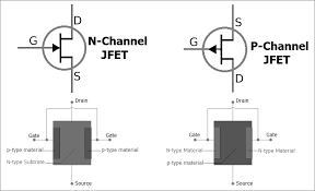
Fig. 1. silicon stack up for P-channel and N-channel JFETs
Steps to perform the real measurement in HP 4145B / Agilent 4156C Semiconductor Parameter Analyzer
- Set up the Agilent 4156C Precision Semiconductor Parameter Analyzer and connect it to the computer with the required software interface.
- Mount the P-channel JFET on the probe station and carefully position the probes on the source, drain, and gate terminals of the JFET.
- Connect the source, drain, and gate terminals to the Agilent 4156C using appropriate connections.
- Configure the Agilent 4156C:
- Set the source-drain voltage (VDS) sweep range (e.g., -10V to 0V).
- Set the reverse bias voltage at the gate-source (VGS) from 0V to a suitable negative value (e.g., 0V to -5V).
- Define the measurement points and ensure the correct sweep rate and compliance settings.
- Turn on the Agilent 4156C and perform the first measurement sweep with VGS set at 0V, recording the IDS (Drain Current) and VDS (Drain-Source Voltage).
- Gradually increase the reverse bias (negative VGS) in small increments (e.g., -1V, -2V, up to -5V) and record the corresponding IDS and VDS for each step.
- Observe and document how increasing reverse bias voltage affects the drain current (IDS).
- Repeat the measurement as necessary for multiple samples to ensure consistency in the results.
- Analyze the collected data to determine the impact of reverse biasing on the P-channel JFET’s performance.
- Turn off the Agilent 4156C and disconnect the setup carefully.
Conclusion:
Summarize the observed effects of reverse bias on the P-channel JFET, specifically noting changes in drain current and voltage characteristics with increasing reverse bias.